Got a package in the mail today. You know what was in it? Nope. But I’ll tell you! Stuff to make better PCBs!
My previous attempts at etching my own circuit boards ended up a little crude to say the least. Using the toner transfer method, perhaps the simplest and cheapest method, my circuit’s traces would melt together, or wouldn’t transfer entirely, so I’d have shorted or broken circuits. Bad stuff. To summarize, it wasn’t pretty, it wasn’t accurate, it really wasn’t workable. When you have to attempt it three or four times to get one that actually is workable, it’s not worth the effort anymore.
Needless to say, I got tired of it sucking. Yes, yes, I know. Some people have very good results with the toner transfer method, some people never have traces melt together, or incomplete transfers. I cannot say that I have EVER had any of my boards come out right. Most of the time, I do it several times over, and it comes out marginally passable. So, I moved up to the next step. I’m now doing etching with photo resist.
Now I print my design on a transparency, place it over a PCB with a photosensitive chemical on it, and expose it to UV light for a few minutes. After that, I take the exposed board, and place it in developer. The developer removes the chemical in the areas exposed to UV. Leaving the stuff behind protected by the transparency to protect the copper underneath.
Next you take the board with the excess photo resist removed and place it in Ferric Chloride. This removes all of the unprotected copper.
Once that’s done, simply wash off the photo resist with some rubbing alcohol, and all of a sudden you’ve got a printed circuit board with traces about as accurate as you can print.
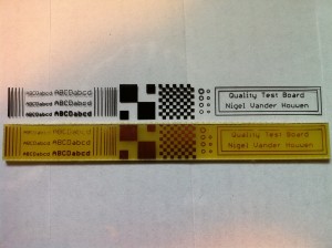
Here’s a photo of a test board I did this evening.
You’ll note that the stuff near the top may have been eaten away a little. There’s kinda two things going on there. One is that I should have exposed the board for a little longer to the UV light. Second is that the top edge of the board after cutting was a little rough, and pushed up on the transparency, since the transparency was lifted up, UV light could get underneath near the top edge, so some of the lines got partially washed away.
You can see however, that there is significant accuracy available. From left to right, there are traces decreasing in thickness down to 0.008 inches, then there’s various sizes and thicknesses of text, then there’s several 0.010 inch traces placed increasingly closely together. Then there’s two checker patterns, to see 1, how well the corners connect, and two how larger areas of protected copper hold up, then there’s holes of various sizes, then is a label with a few long traces run around it to see how well long traces hold up.
Overall I’m very pleased with the results and plan on doing some more testing and creation of actual circuit boards here in the near future to progress some of my projects that have kinda been on hold.
Maybe I’ll even etch some business cards. (Really expensive business cards.)

