
Some time ago I backed a project called Coin that aimed to make a single card that could replace all of your other credit/debit cards. I thought the idea of having all my cards available without having to make room for them in my wallet was a neat idea.
After some time, their team got the device together and shipped out, and I got to use it for myself. I used it for about a month, and quickly came to the conclusion, that it couldn’t replace all my cards, primarily because it didn’t work reliably.
Coin is a bit of tech that tries to digitally pretend to be your selected card as it’s pulled through the stripe reader. It’s a really neat trick, and if it were another industry, it might have worked out better, but when it comes to paying for things, it *HAS* to work, *EVERY* time.
Coin ended up working for me about 75% of the time, which admittedly was pretty cool, but it wasn’t enough of the time that I could pull my other cards out of my wallet. I still needed to be 100% sure I could pay for things, and needing to keep my other cards in my wallet anyway as backup destroyed Coin’s usefulness to me.
Since those days, Coin has sat on my desk, collecting dust, until recently… as you would expect, I finally decided to tear it apart and see what made it tick.
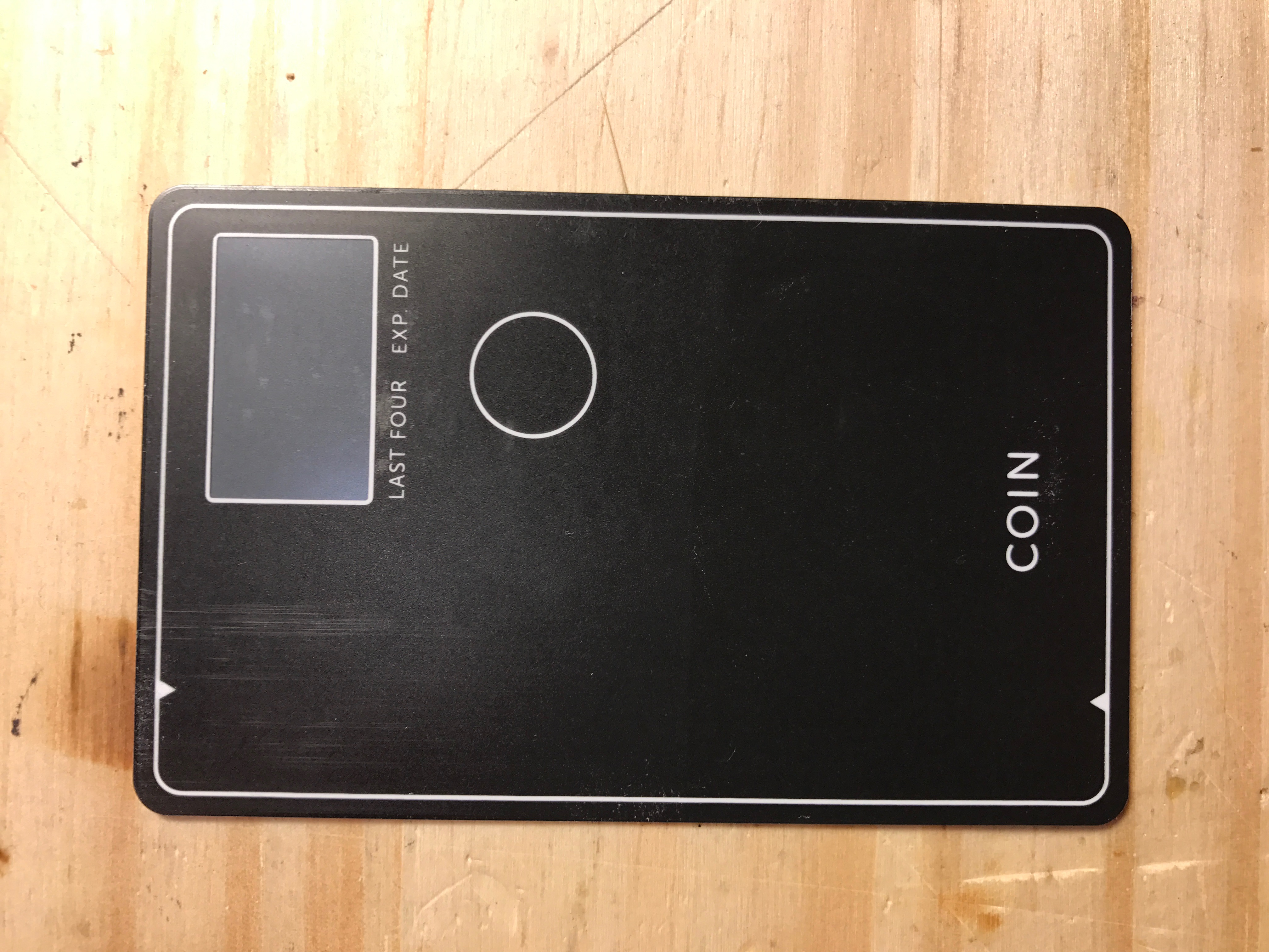
Coin – Pre teardown
The PCB is paper thin, and glued between the plastic front and back. A bit of heat and effort softened the glue and exposed the insides.
On the top, you can see the display, button, and all the components, in addition to the 3V lithium primary cell powering the device (No it’s not rechargeable, but lasts a long long time), as well as the magstripe coils.
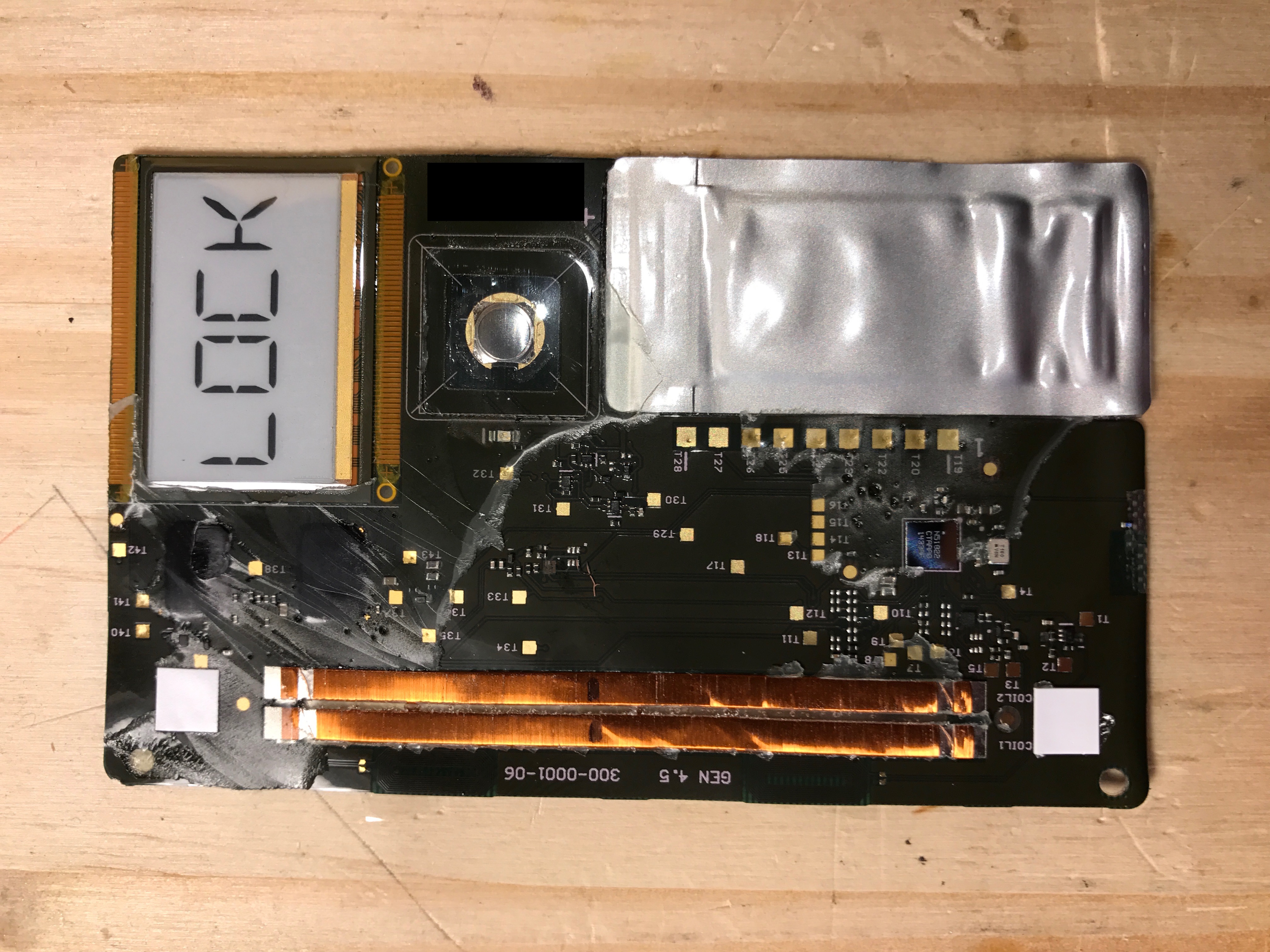
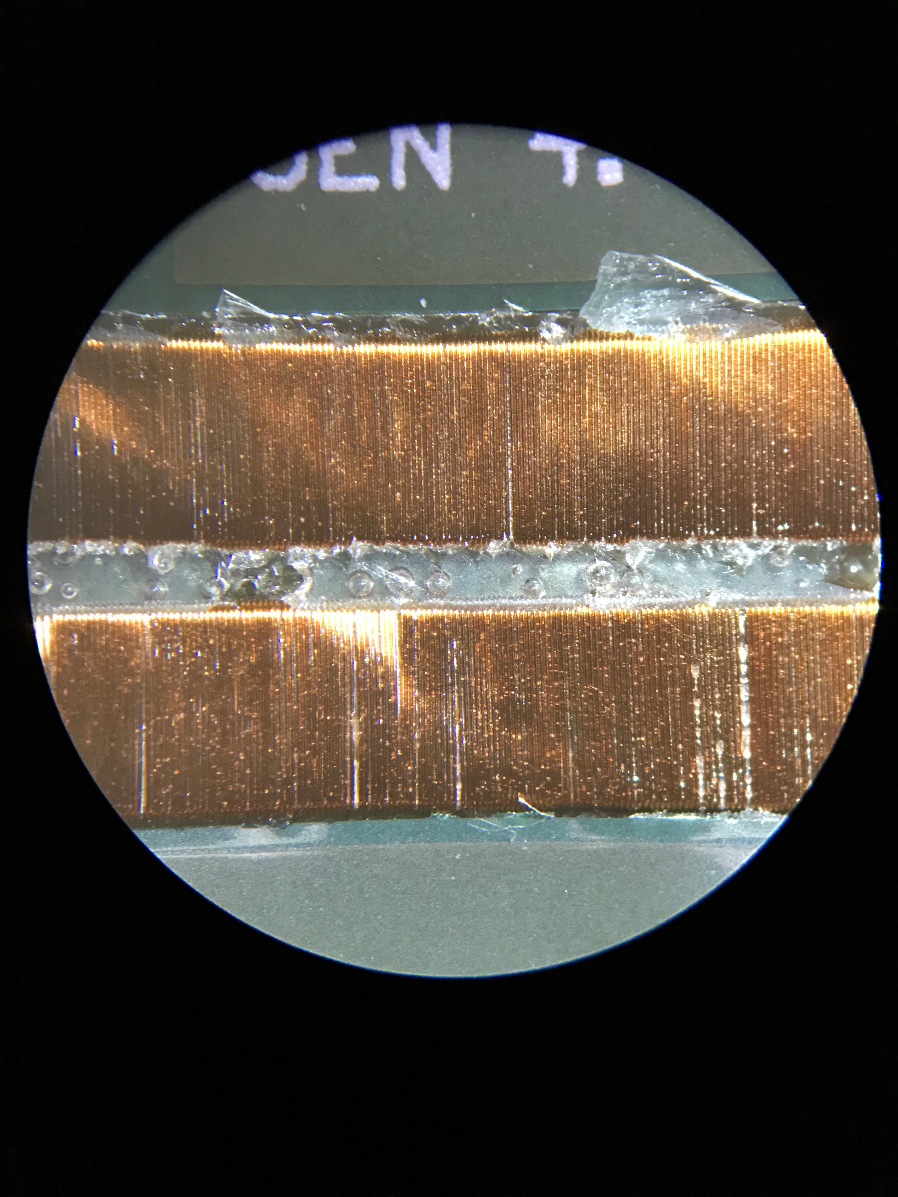
I put it under my microscope to get a closer look at some of the details. Here are the magstripe coils. Looks like it’s just one long coil, not a bunch of individual coils representing the data, so that means Coin is just playing back the bits in sequence like a recording. In theory this would work even if Coin was sitting still in the reader.
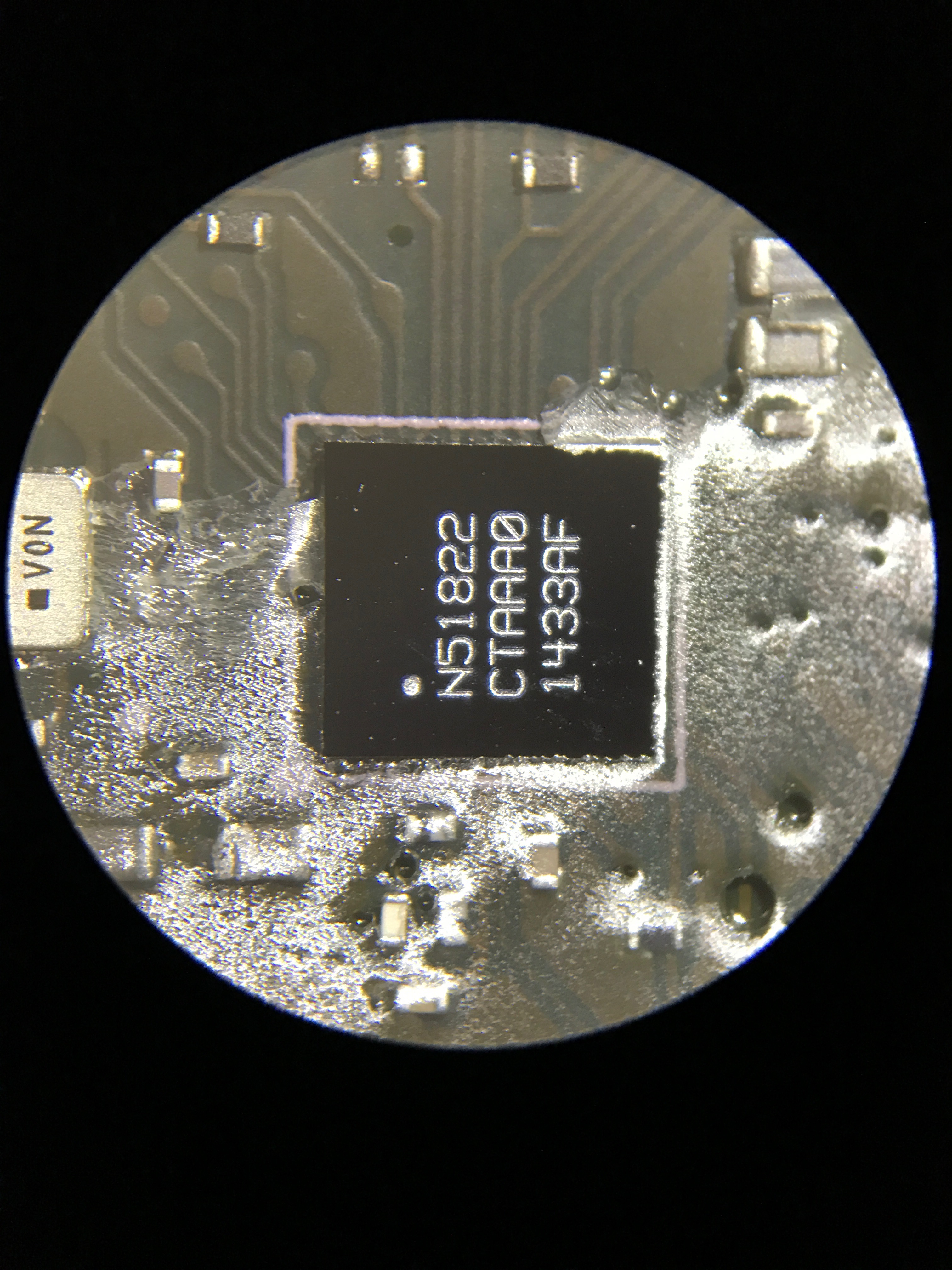
This looks to be the main microcontroller, It’s a Nordic Semiconductor nRF51822 which is specifically designed for very low power applications, and bluetooth connectivity (which Coin uses to talk to your phone.)
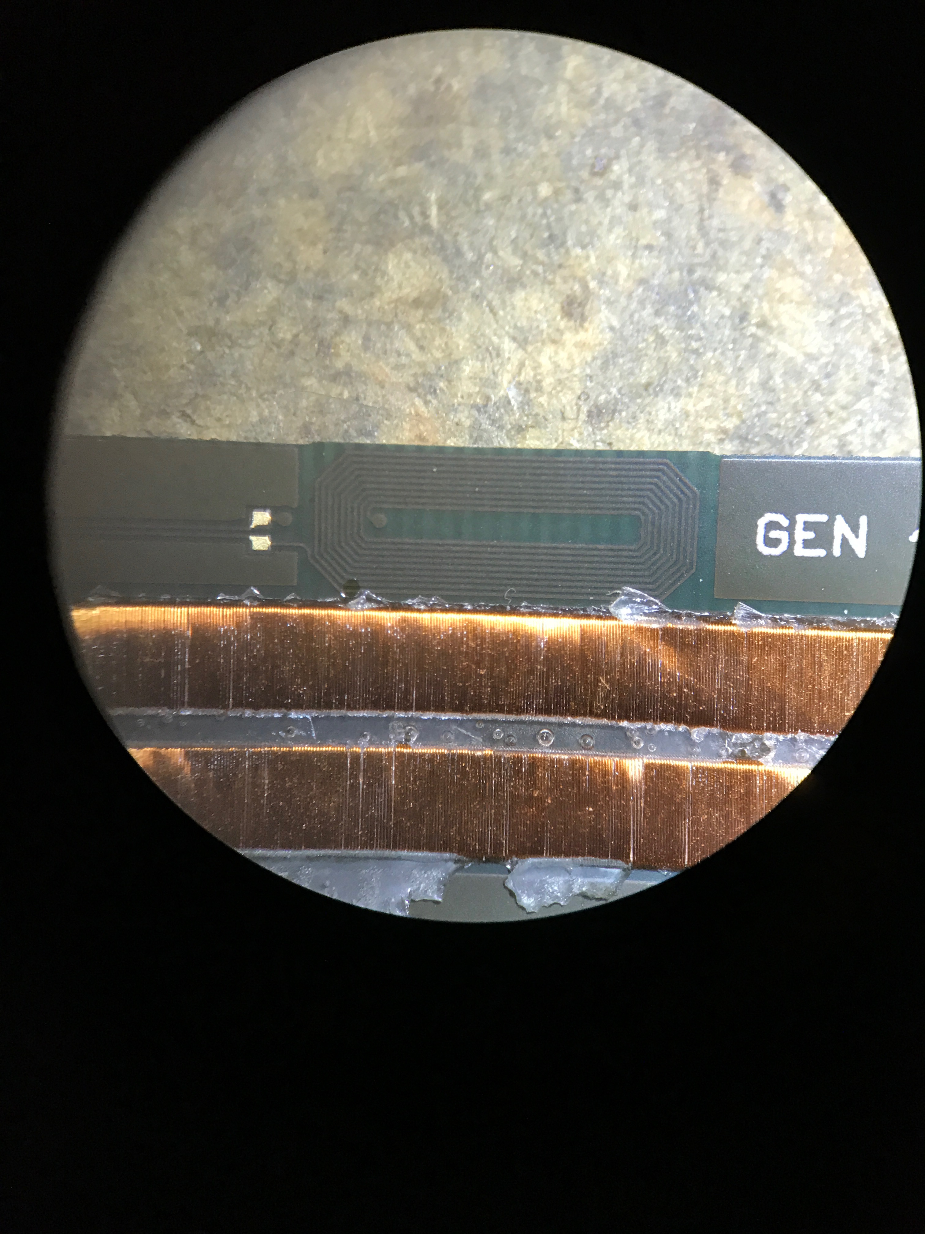
Here we see what I’m guessing is one of the two Bluetooth antennas, stuck out on the edge of the PCB, and the ground plane pulled away a bit.
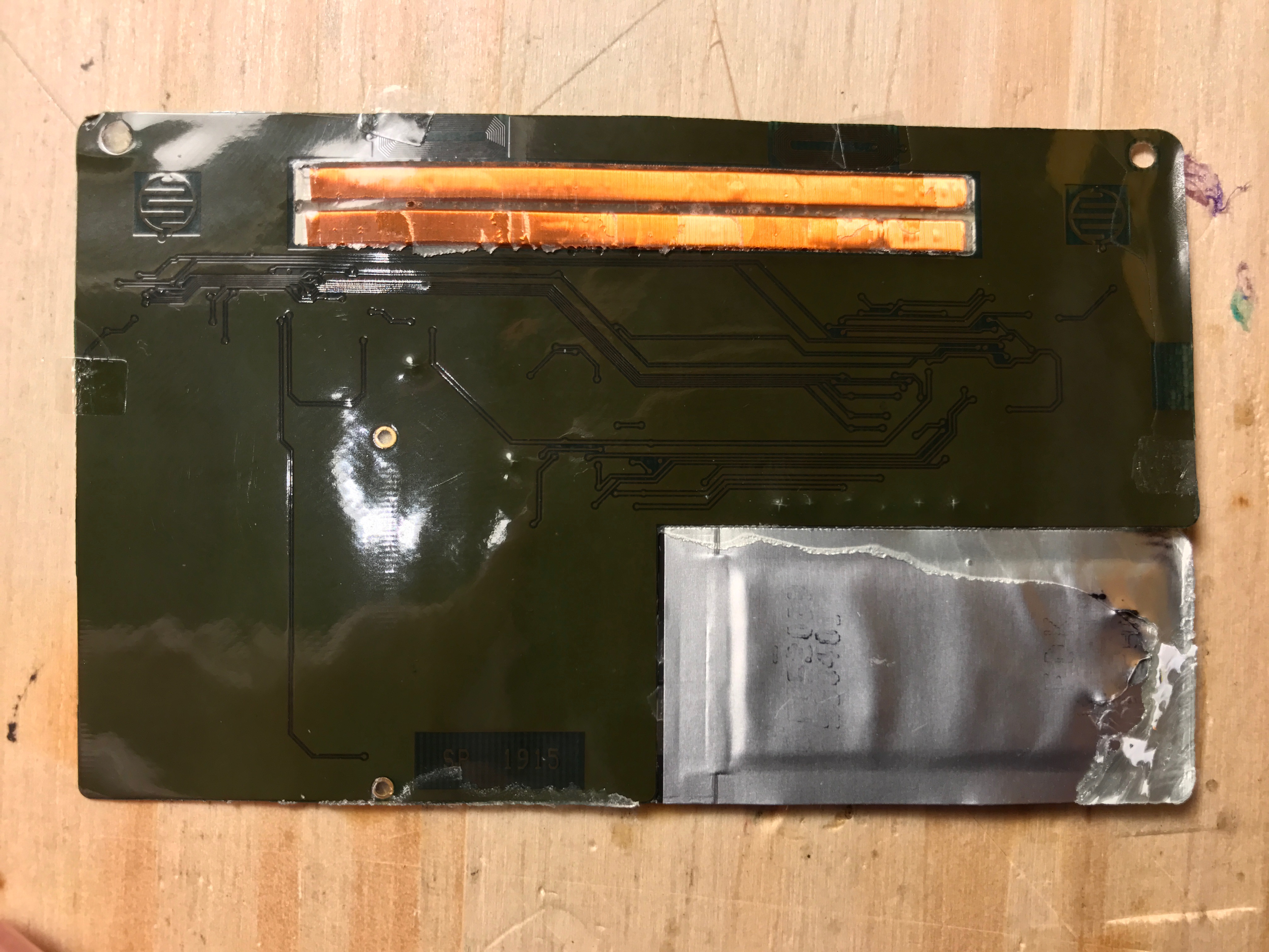
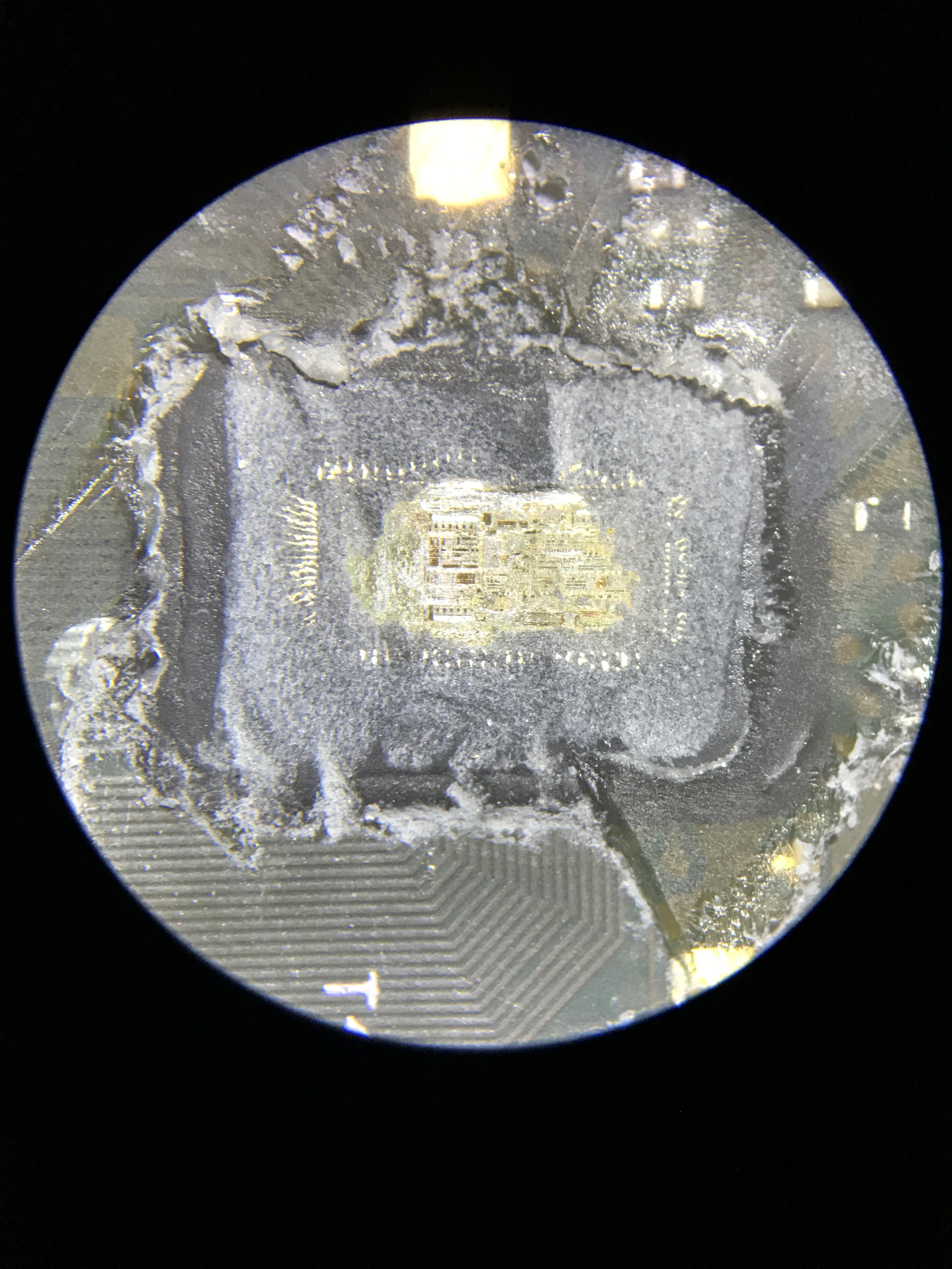
This used to be a Chip-on-Board device before I destroyed it by scraping the black encapsulant off with a knife. You can see the die in the middle, and the gold bond wires around the outside of the die that connect it to the PCB traces. Given the proximity, and where the traces go, I’m betting this is a display driver.
So, in short, a neat bit of tech, a few core components, shoved into a REALLY thin package, and I’m sure a TON of software development and testing time to get it to work as well as it did. Unfortunately it just wasn’t working well enough to be useful to me.
Also, you can see some photos of what I presume is a pre-production device in this FCC filing.
Do you happen to still have this lying around? I’m very interested in how durable it was and what they did to ensure it didn’t break. It is quite hard to find one of these to get your hands on these days though.
No, I tossed it out. In terms of durability, I’d say the biggest advantage it had was the PCB was flexible and would bend easily. At that point, that reduces worries to mostly cracking the solder joints on the parts. Using very small parts (also necessitated by the physical size) helps there as well.
It was a great idea that they took WAY too long to implement. By the time they got it to market about a year later EMV chips and tap to pay were showing up in credit and debit cards pretty much making this thing obsolete. I remember there being talk of them trying to make an EMV version of the coin card, but even now more than a decade later no one has been able to crack and clone an EMV chip card.
Thought of more to add
Today with google pay and apple pay in our phones it also pretty much eliminates this. It might be cool to see google or apple come up with a card somewhat like this but using BLE and NFC to basically emulate how google and apple pay work off your phone for the times when you don’t want to hand off your phone to a server to go ring it up in the back. Go into your wallet app, choose the card you want to pay with using the wallet card then hand off the wallet card for payment.